賴清德副總統出席半導體基地揭牌典禮 肯定培養產業人才即戰力
2023/12/05
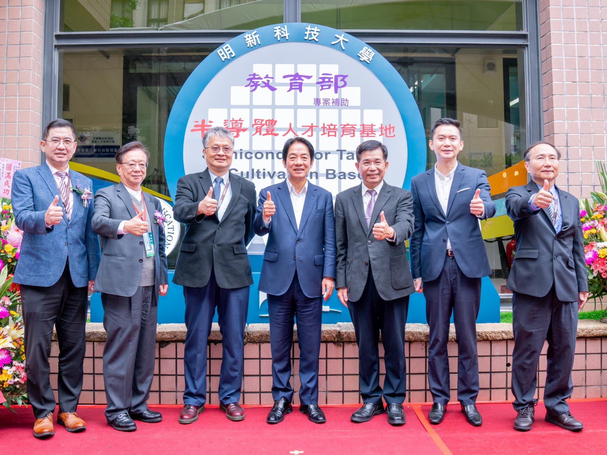
▲半導體人才培育基地啟用,(左起)副校長彭政雄、聯電榮譽副董事長宣明智、校長劉國偉、副總統賴清德、教育部長潘文忠、竹北市長鄭朝方、半導體學院院長張合等人出席揭牌典禮共同為大樓揭牌
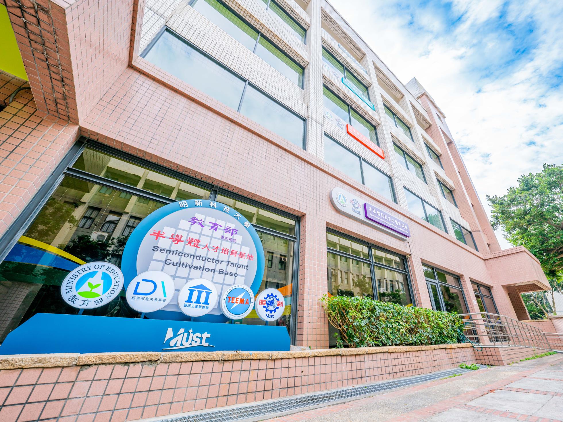
為滿足半導體產業人力需求,本校繼2019年建置全台大學首座「半導體封裝測試類產線示範工廠」、2021年成立首個「半導體學院」後,教育部2022年加碼補助9000萬元,擴大原有規模建置首座以設備廠務與檢測為主的「半導體產業設備廠務與檢測人才培育基地」。此半導體人才培育基地,於12月5日落成啟用,副總統賴清德、教育部長潘文忠、聯電榮譽副董事長宣明智,以及學術、產業界代表等出席為基地揭牌。
副總統賴清德致詞時提到,半導體產業是台灣的優勢,在產官學研合作下有信心持續壯大,不需要擔心因到外國投資而失去優勢。半導體人才培育基地根據產業人才需求來設置,在教育部、科技部及產業界的支持合作下,補助設備、引進業師、縮短學用落差來培養具即戰力的人才。
教育部潘文忠部長表示,配合政府六大新戰略產業及5+2產業創新等重點政策方向,自2022年起推動「建置區域產業人才及技術培育基地計畫」,規劃4年投入新臺幣24億元協助大專校院設置至少20座重點產業人才培育基地,半導體人才培育基地就是大專校院與在地產業及地方政府建立人才合作機制的最佳成果。而創造提升國際競爭力的校園整合平台,一直保持著不遺餘力的持續經營,更隨著少子化搶人資大戰的升溫,打造研討會內化成人才培育連結於政府補助、企業投資案等多贏的孵化器。
劉國偉校長指出,新落成的「半導體產業設備廠務與檢測人才培育基地」是在原來的類產線基地上擴建,面積為原有類產線的4倍大,基地包括「半導體封裝測試類產線」、「半導體廠務類產線」、「半導體設備類產線」、「半導體檢測類產線」,及「半導體測試類產線」共四層樓,樓地板面積約1,100坪,是全台大專院校最大的半導體實務教學基地,在教育部補助及本校追加投資下,整體投入經費前後累積約2億元,從封裝、測試、設備、檢測到廠務,打造如「Mini TSMC」的半導體人才培育基地,提供學生與業界同級廠務環境,全方位培養半導體實務人才。
新成立的基地,除做為教學之用,也可做為企業新人培訓、證照檢定之用,各類產線將針對半導體人力需求,規劃對應的培訓課程,以及與經濟部產業發展署、資訊工業策進會及台灣區電機電子工業同業公會合作,辦理不同階段的證照考試,除原有的「半導體封裝能力鑑定證照考試」,最新審核通過的「半導體測試工程師能力鑑定證照考試」兩張全國唯一半導體證照外,未來將陸續新增「半導體設備工程師能力鑑定證照考試」及「半導體廠務工程師能力鑑定證照考試」,以符合業界所需的各類專業人才。
全新建置的半導體人才培育基地,賴清德副總統與教育部長潘文忠親臨本校為基地揭牌啟用,凸顯政府對台灣產業與人才發展關鍵字「半導體」的高度重視。(半導體學院/提供)
In response to the increasing demand for professionals in the semiconductor industry, Minghsin University of Science and Technology has further expanded its commitment to semiconductor education. After establishing Taiwan's first "Semiconductor Packaging and Testing Factory" in 2019 and founding the country's first "Semiconductor School" in 2021, the university has enlarged its efforts by inaugurating the first "Semiconductor Industry Equipment, Facility, and Testing Talent Cultivation Base (半導體產業設備廠務與檢測人才培育基地) ," focusing primarily on equipment, facilities, and testing. The inauguration ceremony took place on December 5th, with the presence of Vice President Lai Ching-Te (賴清德), Minister of Education Pan Wen-Chung (潘文忠), UMC's Honorary Vice Chair Hsuan Ming-Chih (宣明智), as well as representatives from academia and industry.
In his address, Vice President Lai highlighted the semiconductor industry as a vital asset to Taiwan, expressing confidence in its sustained growth through collaboration between government, industry, and academia. Minghsin Tech's “Semiconductor Talent Cultivation Base” has been strategically set up to address industry needs. With support from the Ministry of Education and industry collaboration, the base receives funding for equipment and attracts industry experts to bridge the gap between academic learning and practical application, cultivating professionals ready for the workforce.
President Liu Kuo-Wei (劉國偉) of Minghsin Tech pointed out that the newly completed "Semiconductor Industry Equipment, Facility, and Testing Talent Cultivation Base" is an expansion of the existing base, occupying four times the original space. The new base includes the original "Semiconductor Packaging and Testing Factory" and adds the "Semiconductor Facility Factory," "Semiconductor Equipment Factory," "Semiconductor Testing Factory," and "Semiconductor Inspection Factory." Covering an area of approximately 1,100 ping, it stands as the largest practical semiconductor teaching base among all universities and colleges in Taiwan. From packaging, testing, equipment, and inspection to facility, it aims to emulate a "Mini TSMC," providing students with real-world semiconductor practice.
The newly established base at Minghsin Tech will not only serve as an educational facility but also as a training ground for new employees in the semiconductor industry and for certification examinations. Various line factories will offer tailored training courses to meet semiconductor manpower needs. Additionally, collaborations with the Industrial Development Administration of the Ministry of Economic Affairs, the Institute for Information Industry, and the Taiwan Electrical and Electronic Manufacturers' Association will facilitate different stages of certification exams. This comprehensive approach aims to nurture a diverse range of professional talents that align with the needs of the industry. (Provided from the Semiconductor School)
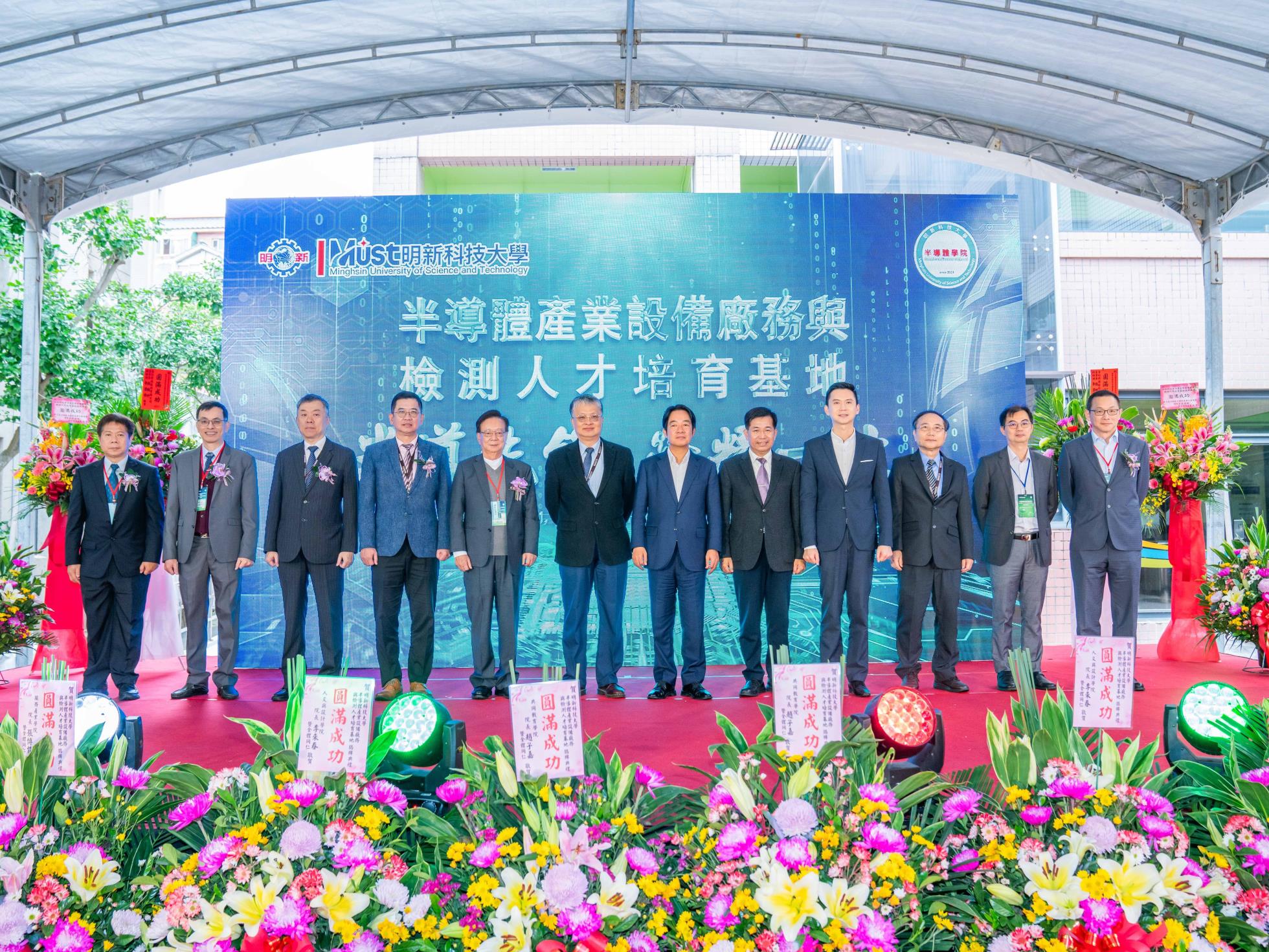
▲明新科大半導體人才培育基地啟用,(左起)矽品副總經理吳禹昇(左起)、美達科技副總經理江敏華、明新科大副校長王舜睦、明新科大副校長彭政雄、聯電榮譽副董事長宣明智、明新科大校長劉國偉、副總統賴清德、教育部長潘文忠、竹北市長鄭朝方、明新科大半導體學院院長張合、台灣半導體研究中心副主任沈昌宏、捷創科技溫在昇副董事長出席揭牌典禮

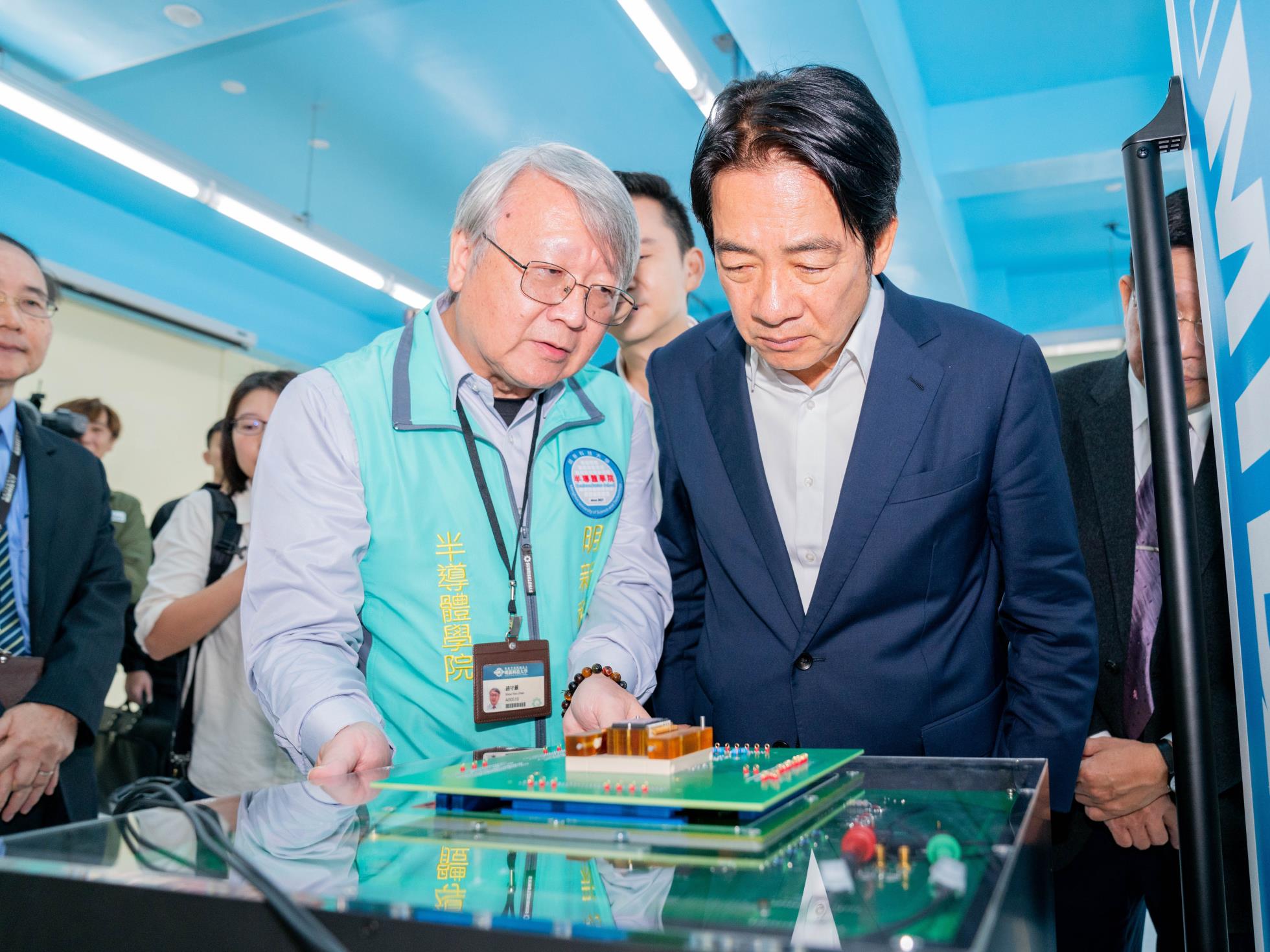
▲明新科大半導體人才培育基地啟用,副總統賴清德(左)親臨揭牌並由明新科大校長劉國偉(右)陪同參觀基地設備
▲副總統賴清德(右)出席明新科大半導體人才培育基地揭牌典禮,並參觀基地設備
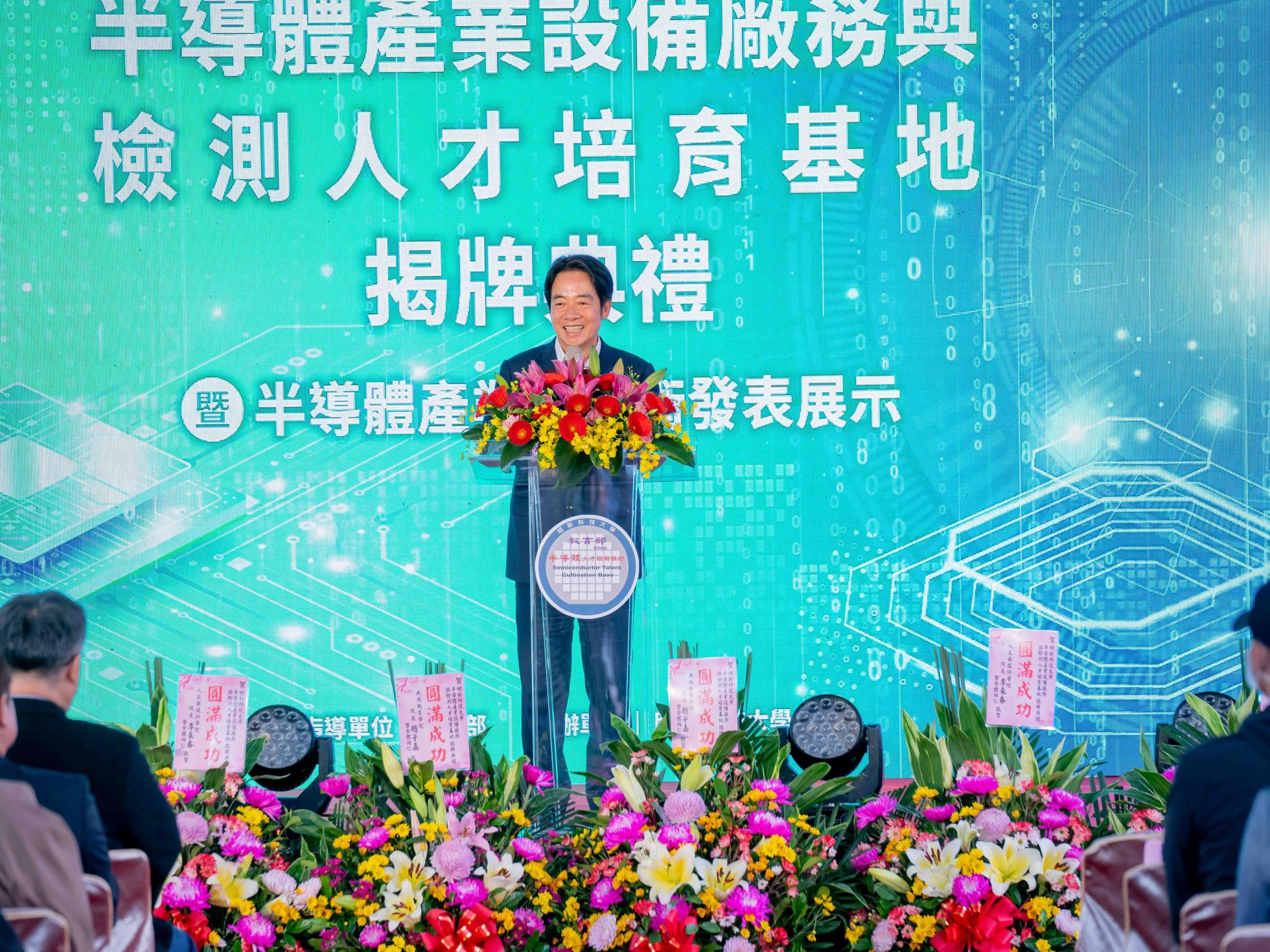
▲副總統賴清德出席明新科大半導體人才培育基地揭牌典禮,肯定基地根據產業人才需求來設置,在教育部、科技部及產業界的支持合作下,補助設備、引進業師、縮短學用落差來培養具即戰力人才的成效
▲明新科大新落成的「半導體產業設備廠務與檢測人才培育基地」是全台大專院校最大的半導體實務教學基地,打造如「Mini TSMC」的半導體人才培育基地,提供學生與業界同級廠務環境,全方位培養半導體實務人才